- 功能建模和信息流建模
- 功能建模和信息流建模(1)
- MongoDB-数据建模
- MongoDB数据建模
- MongoDB数据建模(1)
- MongoDB-数据建模(1)
- 时间序列-建模(1)
- 时间序列-建模
- 数据仓库建模
- 数据流建模(1)
- 数据流建模
- Neo4j数据建模
- Neo4j数据建模(1)
- 威胁建模(1)
- 威胁建模
- 数据仓库什么是维建模
- 数据仓库什么是维建模(1)
- DocumentDB-数据建模
- DocumentDB-数据建模(1)
- UML-建模类型(1)
- UML-建模类型
- 维度数据建模
- 维度数据建模(1)
- 开关级别建模(1)
- 开关级别建模
- 建模与仿真-数据库(1)
- 建模与仿真-数据库
- 机械系统建模
- 机械系统建模(1)
📅 最后修改于: 2021-01-11 14:57:35 🧑 作者: Mango
门级建模
在Verilog中,大多数数字设计都是在更高的抽象水平(如RTL)下完成的。但是,通过使用诸如AND和OR之类的组合元素,在较低的水平上构建较小的确定性电路变得很自然。
在此级别进行的建模称为门级建模,因为它涉及门,并且在硬件原理图和Verilog代码之间具有一对一的关系。
Verilog支持一些称为原语的基本逻辑门,因为它们可以实例化,例如模块,并且它们已经预定义。
门级建模实际上是最低的抽象级别,因为很少使用开关级抽象。门级建模用于实现设计中的最低级模块,例如多路复用器,全加器等。Verilog具有所有基本门的门原语。
Verilog支持内置的基本门建模。支持的门是多输入,多输出,三态和下拉门。
多输入门是and,nand,or,nor,xor和xnor ,它们的输入数量是两个或更多,并且只有一个输出。
多输出栅极是BUF而不是其输出是一个或多个,并具有唯一的一个输入端。
语言也支持三态门,包括bufif0,bufif1,notif0和notif1的造型。这些门具有一个输入,一个控制信号和一个输出。
上拉门和下拉门仅具有单个输出。
句法
以下是每种零延迟门的基本语法,例如:
and | nand | or | nor | xor | xnor [instance name] (out, in1, ..., inN);      // [] is optional and | is selection
buf | not [instance name] (out1, out2, ..., out2, input);
bufif0 | bufif1 | notif0 | notif1 [instance name] (outputA, inputB, controlC);
pullup | pulldown [instance name] (output A);
一个结构中也可以有多个同类型门的实例,用逗号隔开:
and [inst1] (out11, in11, in12), [inst2] (out21, in21, in22, in23), [inst3] (out31, in31, in32, in33);
当电路是简单的组合(例如多路复用器)时,门级建模非常有用。多路复用器是一种将许多输入之一连接到输出的简单电路。
门基元
门原语是Verilog中预定义的模块,可以随时使用。门基元有两类:
- 单输入门原语
- 多个输入门原语
1.单输入门原语
单输入门原语具有单输入和一个或多个输出。门原语not,buf, notif和bufif也具有控制信号。
门仅在控制信号有效时传播,否则输出为高阻抗状态。
1.1不是,buf Gates
这些门只有一个标量输入,但可能有多个输出。
buf代表一个缓冲区,将值从输入传输到输出,而不会改变极性。
并不代表将输入信号极性反转的反相器。因此,其输入为0时将产生1,反之亦然。
句法
module gates (    input a, b,
                output c, d);

    buf (c, a, b);     // c is the output, a and b are inputs
      not (d, a, b);    // d is the output, a and b are inputs

endmodule
例
module tb;
   reg a, b;
   wire c, d;
   integer i;
gates u0 ( .a(a), .b(b), .c(c), .d(d));
   initial begin
    {a, b} = 0;
   $monitor ("[T=%0t a=%0b b=%0b c(buf)=%0b d(not)=%0b", $time, a, b, c, d);
    for (i = 0; i < 10; i = i+1) begin
        #1     a <= $random;
            b <= $random;
    end
end
endmodule
1.2 Bufif,Notif Gates
Bufif和notif原语分别是缓冲区和反相器,带有附加控制信号以使输出可通过bufif和notif原语获得。
仅当启用控制信号时,这些门才具有有效输出,并且输出将处于高阻抗状态。
这些有两种版本,一种具有正常的控制极性,由1表示,例如bufif1和notif1。其次是控制极性反转,由0表示,例如bufif0和notif0。
句法
module bufif_notif_gates (output c, d, input a, b);
bufif (c, a, b);   // c is the output, a and b are inputs
notif (d, a, b);  // d is the output, a and b are inputs
endmodule
例
module bufif_notif_gates_tb;
  reg a, b;
  wire c, d;
  bufif_notif_gates Instance0 (c, d, a, b);
  initial begin
    a = 0; b = 0;
 #1 a = 0; b = 1;
 #1 a = 1; b = 0;
 #1 a = 1; b = 1;
  end
  initial begin
    $monitor ("T=%t| a=%b |b=%b| c(bufif)=%b |d(notif)=%b", $time, a, b, c, d);
  end
endmodule
2.多个输入门基元
多个输入门原语包括AND,OR,XOR,NAND,NOR和XNOR 。它们可能有多个输入和一个输出。
2.1与,或,异或门
AND,OR和XOR门需要多个标量输入并产生单个标量输出。
这些原语的参数列表中的第一个终端是输出,输出随任何输入的移位而变化。
句法
module and_or_xor_gates (output c, d, e, input a, b);
  and (c, a, b);   // c is the output, a and b are inputs
  or  (d, a, b);  // d is the output, a and b are inputs
  xor (e, a, b);   // e is the output, a and b are inputs
endmodule
例
module and_or_xor_gates_tb;
reg a, b;
wire c, d, e;
and_or_xor_gates Instance0 (c, d, e, a, b);
 initial begin
   a = 0; b = 0;
   #1 a = 0; b = 1;
   #1 a = 1; b = 0;
   #1 a = 1; b = 1;
 end
 initial begin
   $monitor ("T=%t |a=%b |b=%b |c(and)=%b |d(or)=%b |e(xor)=%b", $time, a, b, c, d, e);
 end
endmodule
1.2 NAND,NOR,XNOR门
上述所有门的反函数为NAND,NOR和XNOR。仅当基元与其逆版本互换时,才重复使用上面相同的设计。
句法
module nand_nor_xnor_gates (output c, d, e, input a, b);
 nand (c, a, b); // c is the output, a and b are inputs
 nor (d, a, b); // d is the output, a and b are inputs
 xnor (e, a, b); // e is the output, a and b are inputs
endmodule
例
module nand_nor_xnor_gates_tb;
reg a, b;
wire c, d, e;
nand_nor_xnor_gates Instance0 (c, d, e, a, b);
  initial begin
    a = 0; b = 0;
 #1 a = 0; b = 1;
 #1 a = 1; b = 0;
 #1 a = 1; b = 1;
end
  initial begin
    $monitor ("T=%t |a=%b |b=%b |c(nand)=%b |d(nor)=%b |e(xnor)=%b", $time, a, b, c, d, e);
  end
endmodule
所有这些门也可能有两个以上的输入。
module all_gates (output x1, y1, z1, x2, y2, z2 , input a, b, c, d);
  and (x1, a, b, c, d);   // x1 is the output, a, b, c, d are inputs
  or  (y1, a, b, c, d);  // y1 is the output, a, b, c, d are inputs
  xor (z1, a, b, c, d);   // z1 is the output, a, b, c, d are inputs
  nand (x2, a, b, c, d); // x2 is the output, a, b, c, d are inputs
  nor (y2, a, b, c, d); // y2 is the output, a, b, c, d are inputs
  xnor (z2, a, b, c, d); // z2 is the output, a, b, c, d are inputs
endmodule
多路复用器的门级建模
4×1多路复用器的门级电路图如下所示。用于编写4×1多路复用器的模块。
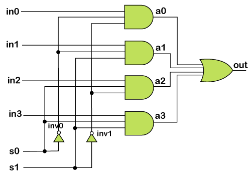
module 4x1_mux (out, in0, in1, in2, in3, s0, s1);

// port declarations
output out; // Output port.
input in0, in1, in2. in3; // Input ports.
input s0, s1; // Input ports: select lines.

// intermediate wires
wire inv0, inv1; // Inverter outputs.
wire a0, a1, a2, a3; // AND gates outputs.

// Inverters.
not not_0 (inv0, s0);
not not_1 (inv1, s1);

// 3-input AND gates.
and and_0 (a0, in0, inv0, inv1);
and and_1 (a1, in1, inv0, s1);
and and_2 (a2, in2, s0, inv1);
and and_3 (a3, in3, s0, s1);

// 4-input OR gate.
or or_0 (out, a0, a1, a2, a3);

endmodule
全加器的门级建模
这是使用半加法器的全加法器的实现。
1.半加法器
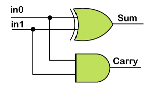
module half_adder (sum, carry, in0, in1);

output sum, carry;
input in0, in1;

// 2-input XOR gate.
xor xor_1 (sum, in0, in1);

// 2-input AND gate.
and and_1 (carry, in0, in1);

endmodule
2.全加器
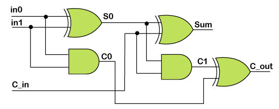
module full_adder (sum, c_out, ino, in1, c_in);

output sum, c_out;
input in0, in1, c_in;

wire s0, c0, c1;
// Half adder: port connecting by order.
half_adder ha_0 (s0, c0, in0, in1);

// Half adder : port connecting by name.
half_adder ha_1 (.sum(sum),
                .in0(s0),
                .in1(c_in),
                .carry(c1));

// 2-input XOR gate, to get c_out.
xor xor_1 (c_out, c0, c1);

endmodule