- 数字逻辑中的移位寄存器(1)
- 数字逻辑中的移位寄存器
- 数字电子中的移位寄存器(1)
- 数字电子中的移位寄存器
- 数字电路-移位寄存器(1)
- 数字电路-移位寄存器
- COA |移位寄存器
- 数字电路-移位寄存器的应用
- 数字电路-移位寄存器的应用(1)
- 数字逻辑中的通用移位寄存器
- 数字逻辑中的通用移位寄存器(1)
- 组移位字符串
- 组移位字符串(1)
- 数字寄存器(1)
- 数字寄存器
- 数组移位 javascript (1)
- 数组移位 javascript 代码示例
- 数据框移位python代码示例
- 计算机寄存器
- 计算机寄存器(1)
- Java中的移位运算符
- Java中的移位运算符(1)
- c#寄存器写入值 - C#(1)
- Vim-寄存器
- Vim-寄存器(1)
- 数组java代码示例中的移位元素
- 二进制寄存器数据
- c#寄存器写入值 - C#代码示例
- 汇编-寄存器
📅 最后修改于: 2021-01-11 15:14:53 🧑 作者: Mango
双向移位寄存器
触发器可用于存储二进制数据的单个位(1或0)。但是,要存储多个数据位,我们需要多个触发器。将连接N个触发器以存储n位数据。
寄存器是用于存储此类信息的设备。它是一组串联连接的触发器,用于存储多个数据位。
这些寄存器中存储的信息可以使用移位寄存器进行传输。
移位寄存器是级联的触发器,其中一个触发器的输出引脚q连接到下一个数据输入引脚(d)。因为所有触发器都在同一时钟上工作,所以存储在移位寄存器中的位阵列将移位一个位置。
例如,如果一个5位右移寄存器的初始值为10110,并且将移位寄存器的输入绑定为0,则下一个模式将为01011,下一个模式将为00101。
双向移位寄存器是能够根据所选模式向右或向左移位数据的存储设备。
下图显示了具有串行数据加载和检索功能的n位双向移位寄存器。最初,通过将其清除引脚驱动为高电平来复位寄存器中的所有触发器。
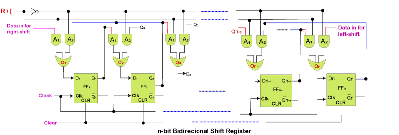
R / L控制线设置为低电平或高电平,以分别选择数据位的左移或右移。
可以通过连接n个触发器来形成n位移位寄存器,其中每个触发器都存储单个数据位。
将这些位向左移位的寄存器称为向左移位寄存器。将向右移位的寄存器称为向右移寄存器。移位寄存器基本上有四种类型,例如:
- 串行输入串行输出移位寄存器
- 串行输入并行输出移位寄存器
- 并行输入串行输出移位寄存器
- 并行输入并行输出移位寄存器
例
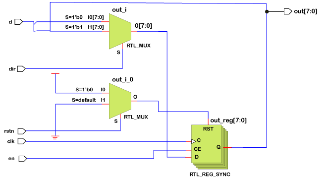
在此移位寄存器示例中,我们采用五个输入和一个n位输出,并使用参数MSB对设计进行参数化,以表示移位寄存器的宽度。
如果n为4,则它将成为4位移位寄存器。如果n为8,则它将成为8位移位寄存器。该移位寄存器具有一些关键功能:
- 可以通过驱动en引脚来启用或禁用它。
- 驱动dir时,它可以左右移动。
- 如果将rstn拉低,它将复位移位寄存器,并且输出将变为0。
- 移位寄存器的输入数据值可以通过d引脚控制。
module shift_reg  #(parameter MSB=8) (  input d,               // Declare input for data to the first flop in the shift register
                                        input clk,                    // Declare input for the clock to all flops in the shift register
                                        input en,                     // Declare input for enable to switch the shift register on/off
                                        input dir,                    // Declare input to shift in either left or right direction
                                        input rstn,                   // Declare input to reset the register to a default value
                                        output reg [MSB-1:0] out);    // Declare output to read out the current value of all flops in this register


   // This always block will "always" be triggered on the rising edge of the clock
   // Once it enters the block, it will first check to see if reset is 0 and if yes, then reset register
   // If no, then check to see if the shift register is enabled
   // If no => maintain previous output. If yes, then shift based on the requested direction

   always @ (posedge clk)
      if (!rstn)
         out <= 0;
      else begin
         if (en)
            case (dir)
               0 :  out <= {out[MSB-2:0], d};
               1 :  out <= {d, out[MSB-1:1]};
            endcase
         else
            out <= out;
      end
endmodule
硬件原理图
试验台
测试平台用于验证该移位寄存器的功能。该示例被实例化到顶层模块中,并且输入具有不同的值。可以在输出OUT引脚被观察到每一个输入的行为。
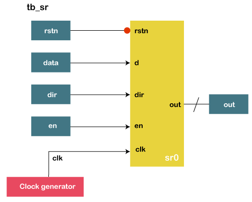
module tb_sr;
   parameter MSB = 16;        // [Optional] Declare a parameter to represent number of bits in shift register

   reg data;                  // Declare a variable to drive d-input of design
   reg clk;                   // Declare a variable to drive clock to the design
   reg en;                    // Declare a variable to drive enable to the design
   reg dir;                   // Declare a variable to drive direction of shift register
   reg rstn;                  // Declare a variable to drive reset to the design
   wire [MSB-1:0] out;        // Declare a wire to capture output from the design

   // Instantiate design (16-bit shift register) by passing MSB and connect with TB signals
   shift_reg  #(MSB) sr0  (  .d (data),
                             .clk (clk),
                             .en (en),
                             .dir (dir),
                             .rstn (rstn),
                             .out (out));

   // Generate clock time period = 20ns, freq => 50MHz
   always #10 clk = ~clk;

   // Initialize variables to default values at time 0
   initial begin
      clk <= 0;
      en <= 0;
      dir <= 0;
      rstn <= 0;
      data <= 'h1;
   end

   // Drive main stimulus to the design to verify if this works
   initial begin

      // 1. Apply reset and deassert reset after some time
      rstn <= 0;
      #20 rstn <= 1;
          en <= 1;

      // 2. For 7 clocks, drive alternate values to data pin
      repeat (7) @ (posedge clk)
         data <= ~data;

     // 3. Shift direction and drive alternate value to data pin for another 7 clocks
      #10 dir <= 1;
      repeat (7) @ (posedge clk)
         data <= ~data;

      // 4. Drive nothing for the next 7 clocks, allow shift register to shift based on dir simply
      repeat (7) @ (posedge clk);

      // 5. Finish the simulation
      $finish;
   end

   // Monitor values of these variables and print them into the log file for debug
   Initial
      $monitor ("rstn=%0b data=%b, en=%0b, dir=%0b, out=%b", rstn, data, en, dir, out);
endmodule
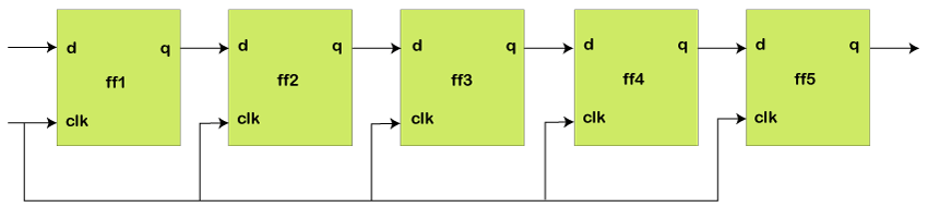
串行输入串行输出移位寄存器(SISO)
允许串行输入(通过一条数据线一个接一个地输入)并产生串行输出的移位寄存器称为串行输入串行输出移位寄存器。
由于只有一个输出,因此数据以串行模式同时离开移位寄存器一位,因此名称为“串行输入串行输出移位寄存器”。
下面给出的逻辑电路显示了一个串行输入串行输出移位寄存器。该电路由四个串联的D触发器组成。
所有这些触发器都是同步的,因为在每个触发器上都施加了相同的时钟信号。
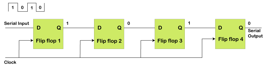
上面的电路是一个右移寄存器的例子,它从触发器的左侧获取串行数据输入。 SISO的主要用途是充当延迟元素。
串行输入并行输出移位寄存器(SIPO)
允许串行输入(通过一条数据线一个接一个地)并产生并行输出的移位寄存器称为串行输入并行输出移位寄存器。
下面给出的逻辑电路显示了一个串行并行并行移位寄存器。该电路由四个相连的D触发器组成。
连接了清除(CLR)信号,并将时钟信号连接到所有4个触发器以将其复位。第一个触发器的输出连接到下一个触发器的输入,依此类推。
所有这些触发器都是同步的,因为在每个触发器上都施加了相同的时钟信号。
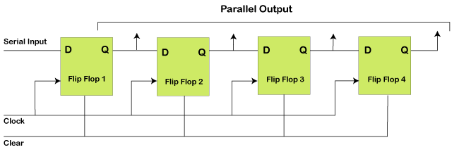
上面的电路是一个右移寄存器的例子,它从触发器的左侧获取串行数据输入并产生并行输出。
它们用于需要将数据线多路分解为几条并行线的通信线路,因为SIPO寄存器的主要用途是将串行数据转换为并行数据。
并行输入串行输出移位寄存器(PISO)
允许并行输入(数据分别分别提供给每个触发器并同时提供给它)并产生串行输出的移位寄存器称为并行输入串行输出移位寄存器。
下面给出的逻辑电路显示了一个并行输入-串行输出移位寄存器。该电路由四个相连的D触发器组成。
时钟输入直接连接到所有触发器。输入数据仍然通过每个触发器输入处的多路复用器分别连接到每个触发器。
前一个触发器的输出和并行数据输入连接到MUX输入,MUX的输出连接到下一个触发器。
由于将相同的时钟信号施加到每个触发器,所以所有这些触发器都是同步的。
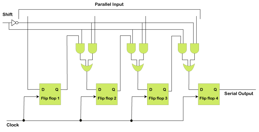
并行输入串行输出(PISO)移位寄存器,用于将并行数据转换为串行数据。
并行输入并行输出移位寄存器(PIPO)
移位寄存器允许并行输入(数据分别同时提供给每个触发器)并产生并行输出,称为并行输入并行输出移位寄存器。
下面给出的逻辑电路显示了一个并行输入并行输出移位寄存器。该电路由四个相连的D触发器组成。清除(CLR)信号和时钟信号连接到所有4个触发器。
由于不需要数据的串行移位,因此在这种类型的寄存器中,各个触发器之间没有互连。
数据以相同的方式分别作为每个触发器的输入给出,并且还从每个触发器分别收集输出。
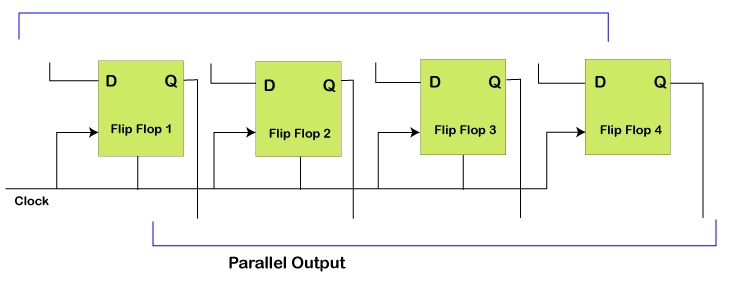
并行输入并行输出(PIPO)移位寄存器用作临时存储设备,并且与SISO移位寄存器一样,它用作延迟元素。
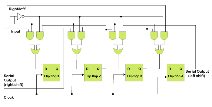
双向移位寄存器
如果将二进制数向左移动一个位置,则等于将数字乘以2。如果将二进制数向右移动一个位置,则等效于将数字除以2。要执行这些操作;我们需要一个可以在任一方向上移动数据的寄存器。
双向移位寄存器是能够根据所选模式向右或向左移位数据的寄存器。
如果选择的模式为1(高),则数据将向右移动;如果选择的模式为0(低),则数据将向左移动。
下面给出的逻辑电路显示了双向移位寄存器。该电路由四个相连的D触发器组成。
输入数据连接在电路的两端,根据选择的模式,只有一个和门处于活动状态。
移位寄存器的应用
这是移位寄存器的以下应用,例如:
- 移位寄存器用于临时数据存储。
- 移位寄存器还用于数据传输和数据处理。
- 串行输入串行输出和并行输入并行输出移位寄存器用于对数字电路产生时间延迟。
- 串行输入并行输出移位寄存器用于将串行数据转换为并行数据。它们用于需要将数据线多路分解为几条平行线的通信线中。
- 并行输入串行输出移位寄存器用于将并行数据转换为串行数据。