pn结二极管-定义,形成,特性,应用
半导体材料的电导率介于导体(例如金属铜)和绝缘体(例如玻璃)的电导率之间。它的电阻率随着温度升高而降低,而金属具有相反的效果。通过在晶体结构中添加杂质(掺杂),可以以有益的方式改变其导电特性。当同一晶体中出现两个不同的掺杂区域时,就会形成半导体结。二极管、晶体管和大多数现代电子产品都建立在电荷载流子的行为之上,例如这些结处的电子、离子和电子空穴。
硅、锗、砷化镓和元素周期表中所谓的准金属阶梯上的元素都是半导体的例子。砷化镓是仅次于硅的第二常见半导体,用于激光二极管、太阳能电池、微波频率集成电路和其他应用。硅是大多数电路生产中的关键组成部分。
pn结
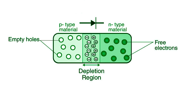
Inside a semiconductor, a p-n junction is an interface or a border between two semiconductor material types, namely the p-type and the n-type.
半导体的 p 侧或正侧具有过量的空穴,而 n 侧或负侧具有过量的电子。掺杂工艺用于在半导体中产生 pn 结。
PN结的形成
当我们利用各种半导体材料形成pn结时,会有一个晶界通过散射电子和空穴来阻止电子从一侧移动到另一侧,这就是我们采用掺杂程序的原因。
例如,考虑一个非常薄的 p 型硅半导体片。如果添加微量的五价杂质,一部分 p 型硅将变为 n 型硅。该片现在将同时具有 p 型和 n 型区域,以及两者之间的结。扩散和漂移是在创建 pn 结之后发生的两种过程。众所周知,结两侧的空穴和电子浓度不同,空穴从p侧扩散到n侧,电子从n侧扩散到p侧。这导致扩散电流流过连接。

当电子从 n 侧扩散到 p 侧时,它会在 n 侧留下一个电离的供体,它是静止的。在结的 n 侧,随着过程的进行,会形成一层正电荷。当一个空穴从 p 侧移动到 n 侧时,一个电离的受主会留在 p 侧,导致在结的 p 侧形成一层负电荷。耗尽区定义为结的每一侧上的正电荷和负电荷区域。由于结的每一侧上的这个正空间电荷区域,产生了从正电荷到负电荷的电场方向。由于电场,结的 p 侧上的电子行进到结的 n 侧。漂移是该运动的名称。我们可以观察到漂移电流与扩散电流方向相反。
pn结二极管的偏置条件
在 pn 结二极管中,有两个工作区域:
- p型
- n型
施加的电压决定了 pn 结二极管的三个偏置条件之一:
- 当 pn 结二极管处于零偏压时,没有外部电压提供给它。
- 正向偏置: p 型连接到电压电位的正极,而 n 型连接到负极。
- 反向偏置: p型连接到电压电位的负端,而n型连接到正端。
前向偏差
The p-n junction is said to be forward-biased when the p-type is connected to the positive terminal of the battery and the n-type to the negative terminal. The built-in electric field at the p-n junction and the applied electric field are in opposing directions when the p-n junction is forward biased.
当两个电场加在一起时,产生的电场小于内建电场。其结果是,耗尽区变得更不抗性和更薄。当施加的电压很高时,耗尽区的电阻变得微不足道。在 0.6 V 时,硅中耗尽区的电阻变得非常微不足道,允许电流在其上自由流动。

反向偏置
The p-n junction is said to be reverse-biased when the p-type is linked to the negative terminal of the battery and the n-type is attached to the positive side. The applied electric field and the built-in electric field are both in the same direction in this situation.
产生的电场与内置电场的方向相同,从而导致电阻更大、耗尽区更厚。如果施加的电压增加,耗尽区变得更耐和更厚。

PN结公式
基于电场产生的内建电位差的pn结公式如下:
E o = V T l n [ N D – N A / n i 2 ]
在哪里,
- 零偏结电压为E 0 。
- 在室温下, V T 是 26 mV 的热电压。
- 杂质浓度用字母N D和N A表示。
- 本征浓度用n i表示
pn结二极管中的电流流动
当电压增加时,电子从结的 n 侧移动到 p 侧。随着电压的升高,空穴从结的 p 侧迁移到 n 侧以类似的方式发生。结果,在两侧的端子之间存在浓度梯度。
由于浓度梯度的发展,电荷载流子会从较高浓度区域移动到较低浓度区域。电路中的电流是由 pn 结内电荷载流子的移动引起的。
V-I Characteristics of PN Junction Diode

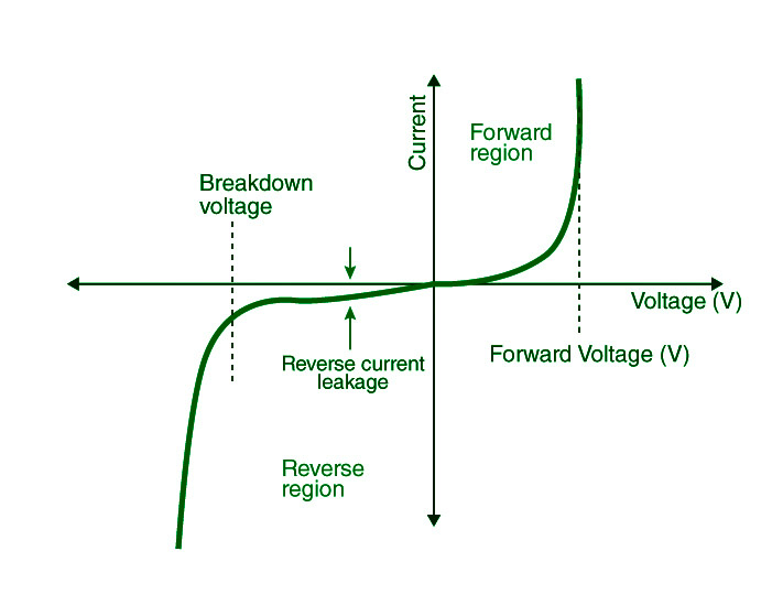
A curve between the voltage and current across the circuit defines the V-I properties of p-n junction diodes. The x-axis represents voltage, while the y-axis represents current. The V-I characteristics curve of the p-n junction diode is shown in the graph above. With the help of the curve, we can see that the diode works in three different areas, which are:
- Zero bias
- Forward bias
- Reverse bias
There is no external voltage provided to the p-n junction diode while it is at zero bias, which implies the potential barrier at the junction prevents current passage.
When the p-n junction diode is in forwarding bias, the p-type is linked to the positive terminal of the external voltage, while the n-type is connected to the negative terminal. The potential barrier is reduced when the diode is placed in this fashion. When the voltage is 0.7 V for silicon diodes and 0.3 V for germanium diodes, the potential barriers fall and current flows.
The current grows slowly while the diode is under forwarding bias, and the curve formed is non-linear as the voltage supplied to the diode overcomes the potential barrier. Once the diode has crossed the potential barrier, it functions normally, and the curve rises quickly as the external voltage rises, yielding a linear curve.
When the PN junction diode is under negative bias, the p-type is linked to the negative terminal of the external voltage, while the n-type is connected to the positive terminal. As a result, the potential barrier becomes higher. Because minority carriers are present at the junction, reverse saturation current occurs at first.
When the applied voltage is raised, the kinetic energy of the minority charges increases, affecting the majority charges. This is the point at which the diode fails. The diode may be destroyed as a result of this.
PN结二极管的应用
- 当pn结二极管的布置被反向偏置时,二极管可以用作光电二极管,因为它对光敏感。
- 它具有用作太阳能电池的潜力。
- 当二极管正向偏置时,它可用于 LED 照明应用。
- 许多电路将其用作整流器,而变容二极管则将其用作压控振荡器。
示例问题
问题一:什么是反向电阻?
回答:
The resistance supplied by a p-n junction diode when it is reverse biased is known as reverse resistance.
问题2:什么是二极管的动态电阻?
回答:
The ratio of change in voltage to change in current is known as dynamic resistance of a diode.
问题3:什么是二极管的静态电阻?
回答:
The ratio of the DC voltage put across the diode to the DC current flowing through it is known as the diode’s static resistance.
问题4:什么是反向偏置?
回答:
When the p-type is connected to the negative terminal of the battery and the n-type is connected to the positive side, the p-n junction is said to be reverse biased. In this case, the applied electric field and the built-in electric field are both pointing in the same direction. Because the generated electric field is in the same direction as the built-in electric field, the depletion zone becomes more resistive and thicker. The depletion region becomes more resistive and thicker as the applied voltage is raised.
问题5:什么是前向偏差?
回答:
When the p-type is linked to the positive terminal of the battery and the n-type to the negative terminal, the p-n junction is said to be forward-biased. When the p-n junction is forward biased, the built-in electric field and the applied electric field are in opposite directions. When both electric fields are put together, the resulting electric field is smaller than the built-in electric field. As a result, the depletion zone grows narrower and less resistive. The resistance of the depletion zone becomes negligible when the applied voltage is large. At 0.6 V, the resistance of the depletion region in silicon is negligible, enabling current to readily flow through it.