- 数字时序电路(1)
- 数字时序电路
- 时序电路介绍(1)
- 时序电路介绍
- 异步时序电路(1)
- 异步时序电路
- 异步时序电路
- 时序电路的VHDL编程(1)
- 时序电路的VHDL编程
- 数字逻辑中的同步时序电路
- 数字逻辑中的同步时序电路(1)
- 组合和时序电路的分析与设计
- 组合和时序电路的分析与设计(1)
- 组合和时序电路的分析与设计(1)
- 组合和时序电路的分析与设计
- 组合电路和时序电路的区别(1)
- 组合电路和时序电路的区别
- 组合电路和时序电路的区别(1)
- 组合电路和时序电路的区别
- 组合电路和时序电路的区别(1)
- 组合电路和时序电路的区别
- 同步和异步时序电路之间的区别
- 同步和异步时序电路之间的区别
- 同步和异步时序电路之间的区别(1)
- 同步和异步时序电路之间的区别(1)
- 同步和异步时序电路之间的区别
- laravel api 路由 - PHP 代码示例
- 弗吉尼亚技术 - 任何代码示例
- Python – GTK+ 3 中的网格容器
📅 最后修改于: 2021-01-12 04:55:32 🧑 作者: Mango
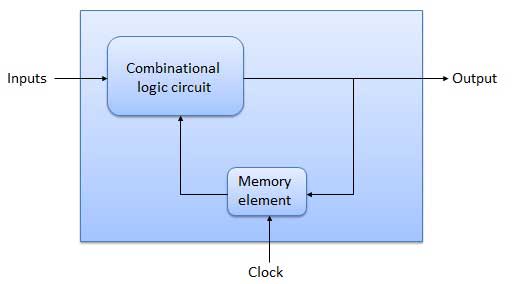
组合电路不使用任何存储器。因此,先前的输入状态对电路的当前状态没有任何影响。但是顺序电路具有存储器,因此输出可以根据输入而变化。这种类型的电路使用先前的输入,输出,时钟和存储元件。
框图
拖鞋
触发器是一种时序电路,通常只在特定的时间采样而不是连续地采样其输入并更改其输出。触发器被认为是边沿敏感或边沿触发的,而不是像锁存器那样被电平触发的。
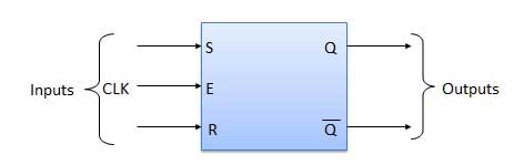
SR触发器
它基本上是SR锁存器,使用带有附加使能输入的NAND门。也称为电平触发的SR-FF。为此,仅当使能输入(E)处于活动状态时,电路才会输出。简而言之,如果E = 1,该电路将用作SR锁存器,但如果E = 0,则输出不变。
框图
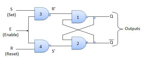
电路原理图
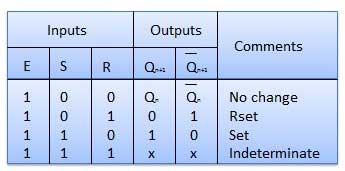
真相表
操作方式
| S.N. | Condition | Operation |
|---|---|---|
| 1 | S = R = 0 : No change |
If S = R = 0 then output of NAND gates 3 and 4 are forced to become 1. Hence R’ and S’ both will be equal to 1. Since S’ and R’ are the input of the basic S-R latch using NAND gates, there will be no change in the state of outputs. |
| 2 | S = 0, R = 1, E = 1 |
Since S = 0, output of NAND-3 i.e. R’ = 1 and E = 1 the output of NAND-4 i.e. S’ = 0. Hence Qn+1 = 0 and Qn+1 bar = 1. This is reset condition. |
| 3 | S = 1, R = 0, E = 1 |
Output of NAND-3 i.e. R’ = 0 and output of NAND-4 i.e. S’ = 1. Hence output of S-R NAND latch is Qn+1 = 1 and Qn+1 bar = 0. This is the reset condition. |
| 4 | S = 1, R = 1, E = 1 |
As S = 1, R = 1 and E = 1, the output of NAND gates 3 and 4 both are 0 i.e. S’ = R’ = 0. Hence the Race condition will occur in the basic NAND latch. |
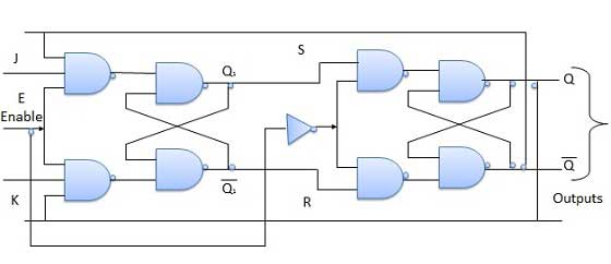
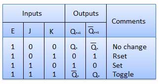
主从JK触发器
主从机JK FF是两个SR FF的级联,具有从第二个输出到第一个输入的反馈。大师是一个积极的触发水平。但是由于时钟线上存在逆变器,从机将响应负电平。因此,当时钟= 1(正电平)时,主机处于活动状态,从机处于非活动状态。而当clock = 0(低电平)时,从机处于活动状态,而主机处于非活动状态。
电路原理图
真相表
操作方式
| S.N. | Condition | Operation |
|---|---|---|
| 1 | J = K = 0 (No change) |
When clock = 0, the slave becomes active and master is inactive. But since the S and R inputs have not changed, the slave outputs will also remain unchanged. Therefore outputs will not change if J = K =0. |
| 2 | J = 0 and K = 1 (Reset) |
Clock = 1 − Master active, slave inactive. Therefore outputs of the master become Q1 = 0 and Q1 bar = 1. That means S = 0 and R =1. Clock = 0 − Slave active, master inactive. Therefore outputs of the slave become Q = 0 and Q bar = 1. Again clock = 1 − Master active, slave inactive. Therefore even with the changed outputs Q = 0 and Q bar = 1 fed back to master, its output will be Q1 = 0 and Q1 bar = 1. That means S = 0 and R = 1. Hence with clock = 0 and slave becoming active the outputs of slave will remain Q = 0 and Q bar = 1. Thus we get a stable output from the Master slave. |
| 3 | J = 1 and K = 0 (Set) |
Clock = 1 − Master active, slave inactive. Therefore outputs of the master become Q1 = 1 and Q1 bar = 0. That means S = 1 and R =0. Clock = 0 − Slave active, master inactive. Therefore outputs of the slave become Q = 1 and Q bar = 0. Again clock = 1 − then it can be shown that the outputs of the slave are stabilized to Q = 1 and Q bar = 0. |
| 4 | J = K = 1 (Toggle) |
Clock = 1 − Master active, slave inactive. Outputs of master will toggle. So S and R also will be inverted. Clock = 0 − Slave active, master inactive. Outputs of slave will toggle. These changed output are returned back to the master inputs. But since clock = 0, the master is still inactive. So it does not respond to these changed outputs. This avoids the multiple toggling which leads to the race around condition. The master slave flip flop will avoid the race around condition. |
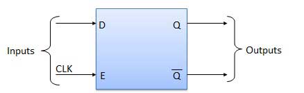
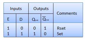
延迟触发器/ D触发器
延迟触发器或延迟触发器是简单的门控SR锁存器,在S和R输入之间连接有NAND反相器。它只有一个输入。一段时间后,输入数据将出现在输出中。由于在i / p和o / p之间存在此数据延迟,因此称为延迟触发器。由于NAND反相器,S和R将彼此互补。因此,S = R = 0或S = R = 1,这些输入条件将永远不会出现。通过SR = 00和SR = 1的条件可以避免此问题。
框图
电路原理图
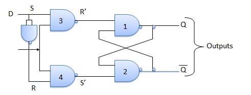
真相表
操作方式
| S.N. | Condition | Operation |
|---|---|---|
| 1 | E = 0 |
Latch is disabled. Hence no change in output. |
| 2 | E = 1 and D = 0 |
If E = 1 and D = 0 then S = 0 and R = 1. Hence irrespective of the present state, the next state is Qn+1 = 0 and Qn+1 bar = 1. This is the reset condition. |
| 3 | E = 1 and D = 1 |
If E = 1 and D = 1, then S = 1 and R = 0. This will set the latch and Qn+1 = 1 and Qn+1 bar = 0 irrespective of the present state. |
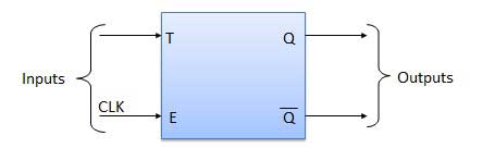
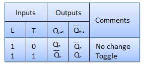
触发器/ T触发器
触发触发器基本上是一个JK触发器,其J和K端子永久连接在一起。如符号图所示,它只有T表示的输入。框图中显示了上升沿触发的T型触发器的符号。
符号图
框图
真相表
操作方式
| S.N. | Condition | Operation |
|---|---|---|
| 1 | T = 0, J = K = 0 | The output Q and Q bar won’t change |
| 2 | T = 1, J = K = 1 | Output will toggle corresponding to every leading edge of clock signal. |